Since Bill de Carle, VE2IQ published his multi-mode beacon keyer circuit in the LOWDOWN, Ive incorporated variations of his design into several homebrew projects. Details of the VE2IQ keyer are found on Bill's web page. This article describes a complete 1-watt LowFER transmitter that can be built on a single 4 by 6 inch board containing a frequency synthesizer, clock reference, keyer and final amplifier. The synthesizer tunes in 100-Hz steps from 130 to 190 kHz, and the built-in identifier provides both Binary Phase-Shift Keying (BPSK) and CW operation.
Additions and corrections (11-20-00): Besides the other corrections noted in the text of the article, I discovered that R13, a 180 ohm resistor was omitted from the parts list. Also, thanks to Don, W2MPK and Jack, K2JDD who caught an error in the original schematic of the synthesizer, keyer and modulator. Resistor R9 should have been connected to pin 4 of U3 rather than to pin 3. The schematic in this article now shows the proper connection point, and the circuit board layout was correct.
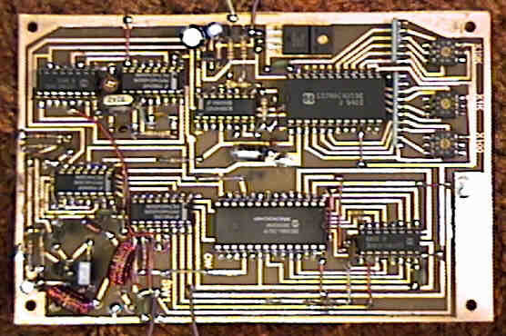
Figure 1 shows a prototype of the all-in-one transmitter, built on a printed circuit board (PCB) that was made with an "iron-on" technique that will be described later. The rotary DIP switches that set the frequency are located in the upper right corner of the board, and the final amplifier (including an output low-pass filter) is in the lower left. In this picture, taken before I had a high-resolution digital camera, it looks like the circuit board extends beyond the shiny outer rectangle of copper, but that is simply because the background is about the same color as the etched portion of the board.
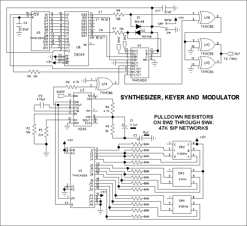
The schematic is shown below and is broken into four blocks. The first
block contains the phase locked loop (PLL) synthesizer, EEPROM-based identifier,
and BPSK/CW modulator. A 4046 CMOS PLL chip is used to generate the carrier
frequency and is programmable by means of miniature binary-coded decimal
(BCD) rotary switches mounted on the PC board. The PLL is the part of the
circuit that can give the most headaches; not because there is anything
exotic about the circuit, but because there seems to be a lot of variation
between chips from different manufacturers. Max Carter had warned in previous
articles in the LOWDOWN that only the 4046 and 74HC4046 chips manufactured
by National Semiconductor can be depended upon to have relatively low phase
noise. My own tests on chips from several sources have confirmed this.
Unfortunately, Digi-Key no longer carries National CMOS parts, and a visit
to the National web page shows that they no longer list any CMOS devices.
Bummer! However, I used a Fairchild 4046 from Digi-Key in the prototype,
and although it sounds pretty bad if you listen to a harmonic in the HF
region, it is stable enough on LF for BPSK operation. Bruce, W0BK has used
the prototype board on his BK beacon from Shell Lake, WI, and has been
copied in BPSK mode by Bill Bowers in Oklahoma and Bill de Carle in Quebec.
The other thing about PLL chips is that they may not cover the desired
tuning range with the component values shown in my diagram. There are two
easy ways to check the tuning range. If you have a frequency counter, connect
it to pin 3 of U1A and attach a test lead to pin 9 of the 4046 (U3). When
the test lead is tied to the +5 volt line (pin 16 of U3), the voltage controlled
oscillator (VCO) in the 4046 will be tuned to the high end of its frequency
range, and with the test lead grounded, the VCO is tuned to its lowest
frequency. These limits must be a few kilohertz beyond the ends of the
desired tuning range for reliable operation. If you dont have a frequency
counter, connect a very high impedance voltmeter or oscilloscope probe
to pin 9 of U3 and set the BCD switches to the lowest desired frequency,
for example 130 kHz. The voltage on pin 9 should be at least 0.5 volts
above ground. With the BCD switches set to 190 kHz, the voltage on pin
9 should be no higher than about 4.5 volts. Use a larger value for C5 to
lower the frequency of the PLL and a smaller value to raise it. If a 74HC4046
is substituted for the CD4046, C5 needs to be considerably larger than
the 470 pF shown in the diagram; probably around 1500 pF.
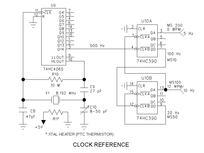
An inexpensive microprocessor crystal is used in the clock reference circuit shown below, with a positive temperature coefficient (PTC) thermistor attached to the crystal to improve the frequency stability. The PTC thermistor serves as both heater and sensor. It isn't necessary to include the thermistor if the transmitter will be operated only in CW mode, but I strongly recommend it for BPSK work. The preferred method for attaching the thermistor to the crystal is to carefully tin one side of the metal crystal can, then carefully unsolder the lead from one side of the thermistor and carefully solder that side to the crystal can. A thin wire is run from one side of the crystal can to ground; the remaining lead of the thermistor is connected to the +5 volt supply. An alternative to soldering the heater to the crystal is to leave the thermistor leads intact and attach it to the crystal can with epoxy, duct tape or your favorite adhesive. I also recommend making a tiny "mitten" out of thin foam packing material and Scotch tape, and slipping it over the crystal/heater combination to form a miniature crystal oven. Not all 8.192 MHz crystals will tune to exactly the right frequency in this circuit, although you're fairly safe if you use the one from radioshack.com that is specified in the parts list.
Those who have seen my article on a "Simple LowFER Transmitter" will recognize the complementary-pair final amplifier circuit below. Small-signal plastic transistors are normally adequate for 1-watt operation, and the ones specified in the parts list should work just fine. However, they are likely to get hot if the antenna is not tuned to resonance (or disconnected). Unlike some other final amplifier circuits, this one is not likely to self-destruct under a badly mismatched load condition, especially if a power limiting circuit is used. Larger transistors like an NTE128/NTE129 pair can also be used in the final amplifier to reduce the probability of overheating (and possibly give better efficiency.)
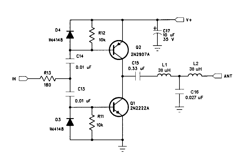
Final Amplifier
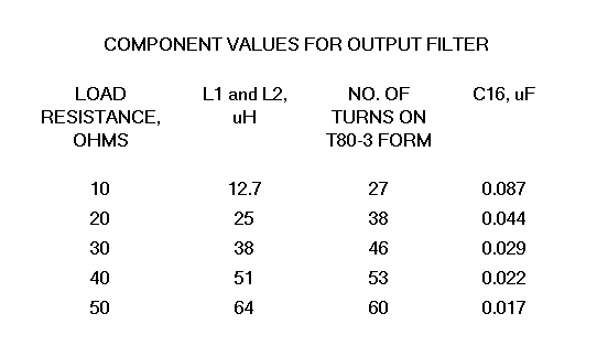
The output filter in this final amplifier circuit differs slightly from the one in my Simple LowFER Transmitter article, in that it is designed to work into a 30 ohm load rather than 50 ohms. This represents a better compromise for most LowFER antennas, since the actual feed impedance of a really good LowFER antenna will be around 10 ohms, and a more typical antenna might have an impedance of 25 or 30 ohms. L1 and L2 are two separate coils, each wound with 46 turns of #26 AWG enameled magnet wire on T80-3 (grey) toroid forms. For other values of load impedance, use the values shown in the table below. Unless you're a real purist, component values for the filter are not critical because a typical LowFER antenna is not a fixed, purely resistive load, and tuning the antenna for maximum output corrects for any "mismatch" in the filter. L1 and L2 can be wound on T50-3, T68-3 or T80-3 forms, and C16 can use the nearest standard capacitor value.
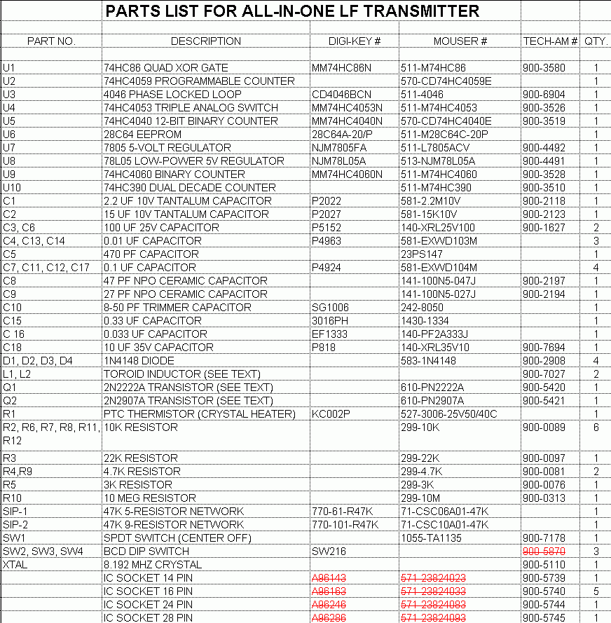
One frustration in homebrew projects is that it is seldom possible to buy all the parts from one or two suppliers, so that you're stuck with minimum order and/or shipping charges from several vendors. This project is no exception. When I first built the all-in-one prototype, I was able to keep it down to two suppliers -- Mouser and RadioShack.com (formerly TechAmerica). If something was out of stock, Digi-Key was there as a backup. The parts list below shows catalog numbers that were correct as of some time in 1999, and most of those numbers should still be valid. Unfortunately, Mouser has stopped carrying the 74HC4059 programmable counter, and the part isn't in the recent Digi-Key or RadioShack.com catalogs either. At last report the CD4059, which can be used in place of the 74HC4059 in this circuit, was available from www.jameco.com as part number 13143.
Recently (July 2000), while trying to order parts for additional copies of the synthesized LowFER transmitter, I discovered two other problems. First, the RadioShack.com BCD DIP switch (RS part number 900-5870) that was shown on the original parts list has a completely different pinout than the Digi-Key switch (No. SW216) I used in the prototype. There is no easy modification to the circuit board that will allow substitution of the Radio Shack switch. Second, AMP has discontinued the surface mount DIP sockets and they are no longer stocked by either Digi-Key or Mouser. Acceptable substitutes are the inexpensive leaf-spring type of IC sockets, but you have to use a needle nose pliers or other type of tool to bend the pins into an "L" shape. High-quality sockets with machined pins won't work because you can't bend the pins at all. Of course, another alternative is to dispense with the IC sockets and bend the IC pins for direct soldering to the PC board. A revised parts list is shown below with the deleted items shown in red. Suggested part numbers for the RadioShack.com IC sockets have been added to the original list.
This circuit can be built using conventional point-to-point wiring, or even on a plug-in protoboard, but the number of interconnections required will make it a fairly tedious task with lots of possibilities for errors. There is also likely to be a lot of "hash" from the digital circuits and the final amplifier, which is likely to get into the PLL circuit. I recommend using a two-sided PC board, with all of the copper left on one side to serve as a ground plane, and with the parts surface mounted on the other side. Making your own PC board, especially one of this complexity, can be a little daunting, but it is possible to do it at home with a minimal investment in equipment. An article entitled "Ironing Out Your Own Printed Circuit Boards" by John Grebenkemper in the July 1993 QST gives the details on how to do it. As the name implies, the technique uses an ordinary household iron to transfer the toner from a laser printout or plain-paper copy of the PCB layout to the copper plating on the circuit board. Actually the toner sticks to the circuit board and the paper stays stuck to the toner, so it's necessary to soak it all in a weak household bleach solution for a few hours to break down the paper. Then the paper is washed off, leaving the toner as a "resist" that keeps the etching solution from attacking the copper in the areas of the traces and pads on the circuit board. Ferric chloride etching solution can be purchased from the local Radio Shack store. There are some commercial iron-on films that can be peeled off as soon as they cool, eliminating the time and mess involved in dissolving away the paper. However, the stuff I've tried tends to peel off areas of toner at the same time, which requires a lot of touching up with a Sharpie or other permanent marking pen. Epson photo quality inkjet paper seems to work better than the commercial films I've tried, and can be washed off after soaking it in warm soapy water. Note: the inkjet paper works fine, but it can't be printed on an inkjet printer; it has to be done on a laser printer or copier. Large areas of copper (including the unetched back side of the board) can be protected from etching with masking tape or clear plastic package sealing tape.
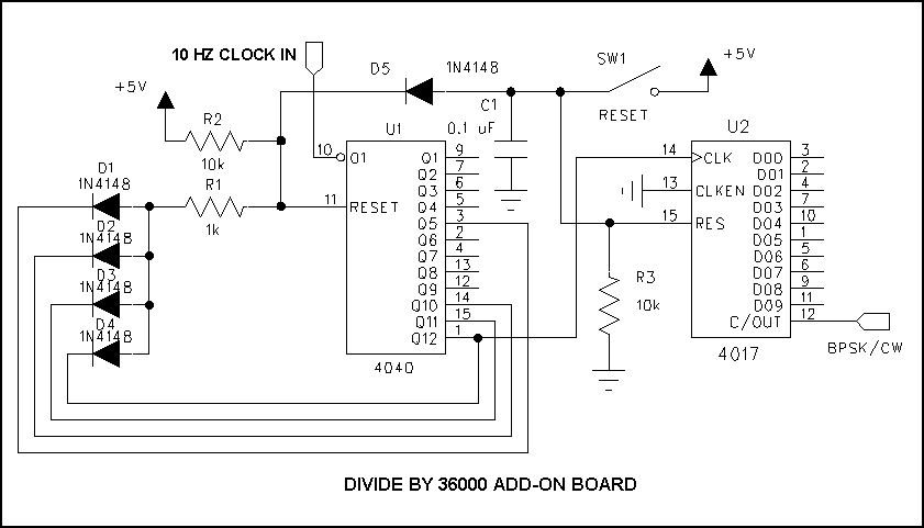
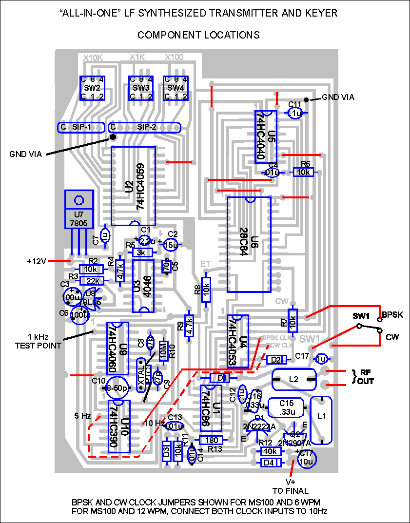
A composite sketch of the circuit board showing the traces, component locations and necessary wire jumpers is included below. Observe the component orientations carefully because some of the integrated circuits are installed "backwards" from the rest in order to simplify the interconnections. Red lines on the layout indicate where external wires or jumpers are required. The BPSK clock jumper is shown connected to the 10 Hz output of clock divider U10, which is the position for MS100 (10 baud) BPSK. A dashed red line is shown connecting the CW clock to the 5 Hz output of U10. This gives a CW keying speed of 6 WPM. I personally prefer 12 WPM for my beacon keying speed, which requires a 10 Hz clock signal, and which can be achieved by leaving out the dashed red jumper and connecting the "BPSK CLK" and "CW CLK" pads together. An external switch SW1 selects either the BPSK or CW mode by applying either +5 volts (BPSK) or grounding (CW) the switched line. A divide by 36,000 add-on option that can be used to switch between BPSK and CW automatically at half-hour intervals is described later.
Ground "vias", which connect the top side to the unetched ground plane on the back side of the board, are required in a couple of locations on the circuit board layout. It is necessary to drill a very small hole at these locations and solder a short wire to the top and bottom sides. I also recommend adding other vias at several points such as at each corner of the board to provide a "solid" ground connection to the backplane. Other than the vias and the mounting holes, no drilling is required. It takes a small iron and some patience to solder the components to the board in "surface mount" style, but it sure beats all that drilling. It's also easier to remove and replace components in the unlikely event (famous last words) that this becomes necessary.
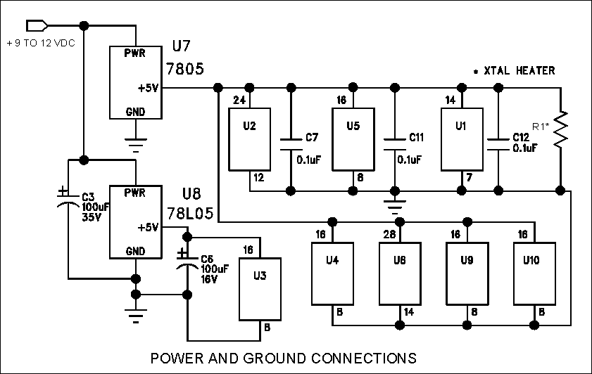
Separate connection points are provided for the DC power input to the logic circuits and the final amplifier. A voltage of +12V is shown on the layout for the logic power supply, although anything between about 8 and 15 volts is within the range of the on-board regulators. Current drain is quite low. I've forgotten the exact numbers but expect that it is well under 100 mA. The V+ supply for the final is adjusted so that the DC power input is 1 watt or less when the antenna is tuned for best output. Typically this will require a voltage between 10 and 15 volts. My LowFER final, which is very similar to the one on this board, works best with my antenna when the supply voltage is 13 volts. I use a 26 volt regulated supply with a 169 ohm, 1 watt resistor in series with the final amplifier's DC input. This limits the power input to 1 watt or less no matter how the antenna is tuned, and also helps to keep the output constant even if the antenna is detuned slightly.
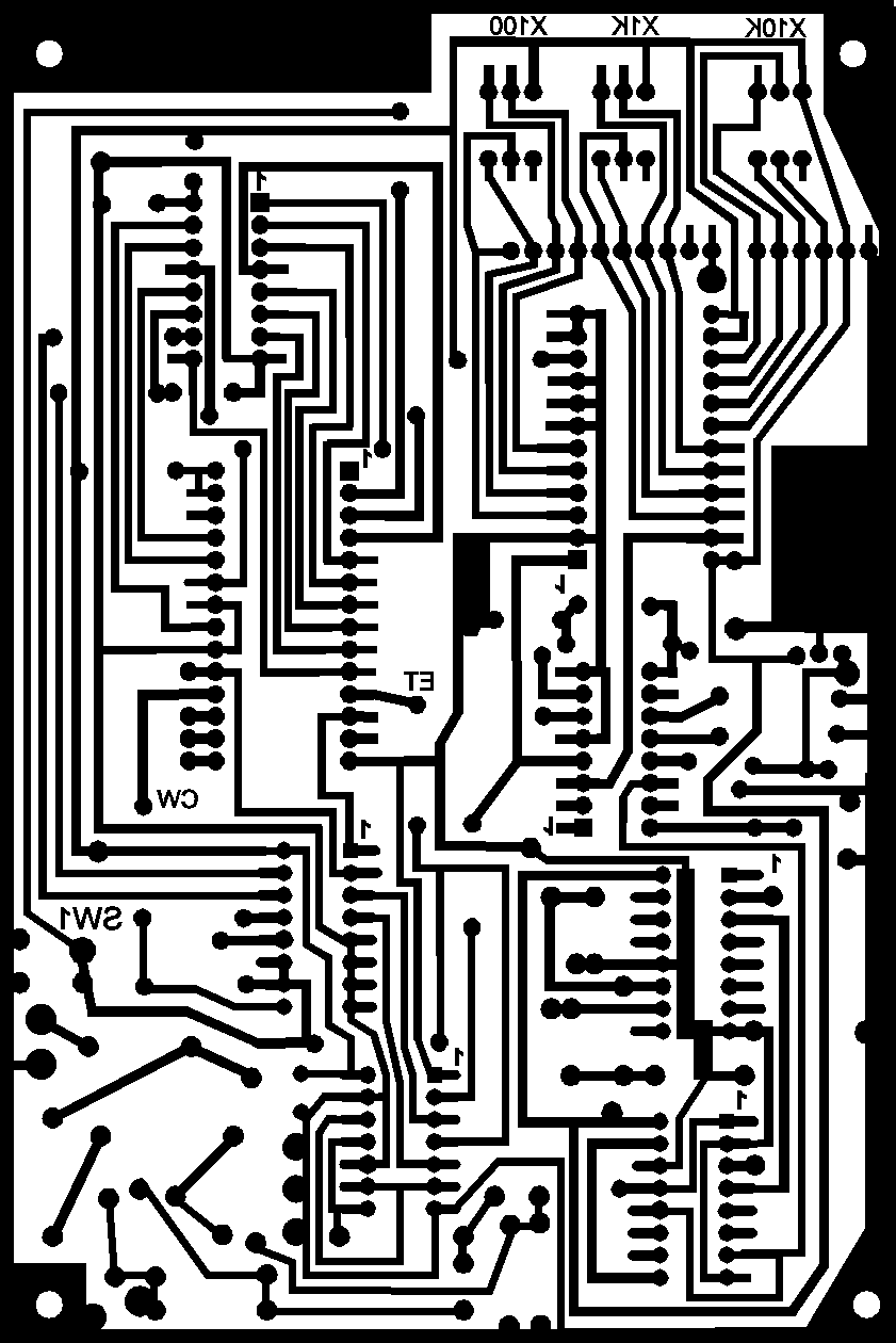
The circuit board pattern is shown below. This is a mirror image of what the actual pattern will look like, so that it will come out correctly when printed or copied and ironed onto the board. It is necessary to re-size this image so that it is exactly 4 inches wide by 6 inches high overall, in order for the component pads to come out with the right dimensions. I'll be happy to send a laser printout of this pattern with the correct dimensions in exchange for a large, stamped, self-addressed envelope.
The heart of this circuit is a 28C64 EEPROM (or 27C64 PROM), which must be programmed with the desired messages. Separate messages can be programmed for BPSK and CW, and both "halves" of the EEPROM must be programmed in order to use both modes. Bill de Carle's web site has a program called MATIC which will allow you to generate the necessary files to use with commercial PROM or EEPROM "burners". Bill's site also includes a schematic for a RAM version of his keyer, which can be used as an EEPROM programmer. I have been using his circuit here for several years, and if someone sends me a 28C64 and return postage, I'll program it with the LowFER beacon messages of his (or her) choice.
There are many more listeners with CW reception capability than BPSK;
however BPSK offers a very significant advantage over CW for weak-signal
conditions (about the only kind of conditions we LowFERs ever see). To
enjoy the best of both worlds, some of us have set up our beacons to send
BPSK and CW alternately on a regular schedule. Switching at half hour intervals
seems to be a good compromise, allowing enough time to "listen" for either
mode and still take advantage of good band conditions (on LF, conditions
usually don't change too rapidly). The circuit below takes the 10 Hz clock
signal from the all-in-one transmitter board and divides it by 36,000 to
provide a square wave output with a one-hour period. This output is fed
to the BPSK/CW switch input on the transmitter board. Closing the "reset"
switch will put the transmitter in the CW mode for exactly half an hour,
and the cycle will repeat at one hour intervals for as long as power is
maintained. I haven't done a PC board layout for this circuit, but it's
simple enough to build on a small protoboard.